Unit 8 — Working with Real Spectral Data: Integration (Data Lab)
Big idea. A spectrum is a table of numbers — irradiance per nanometre at each wavelength. Adding up "height × width" slices (integration) turns it into the totals engineers use: total irradiance, the fraction in any band, photon flux, and the maximum current a given band gap can deliver. You will do this yourself with the real ASTM G173 table.
Learning objectives
- Explain what spectral irradiance (W m⁻² nm⁻¹) means and why you must integrate it.
- Apply the trapezoid rule to unevenly spaced data in a spreadsheet or Python.
- Compute band fractions, photon flux and the maximum short-circuit current \(J_{sc,\max}\) for any band gap.
- Check your numbers against the reference values in this unit.
Why this matters
"What fraction of sunlight can material X use?" and "what is the maximum current of a cell with gap \(E_g\)?" are integrals of the spectrum. Spectral mismatch corrections, quantum-efficiency-to-current calculations, and tandem current matching (SOL 202/203/401) are the same operation with an extra factor inside.
What "per nanometre" means
The G173 table lists, for each wavelength, the irradiance per nanometre of bandwidth. At 500 nm AM1.5G is about 1.55 W m⁻² nm⁻¹ — meaning a 1-nm-wide slice around 500 nm carries about 1.55 W/m². To get the power in a band you add up slices: power = area under the curve.
In words: integrate (sum) the spectral irradiance over the wavelengths you care about.
The data
ASTM G173-03 has 2002 rows from 280 to 4000 nm with columns: wavelength (nm), extraterrestrial (AM0), global tilt (AM1.5G), and direct + circumsolar (AM1.5D), all in W m⁻² nm⁻¹. The spacing is not uniform: 0.5 nm from 280–400 nm, 1 nm from 400–1700 nm, then 5 nm to 4000 nm (with a short transition). Any method that assumes equal spacing will be wrong.
Where to get it: the NREL (now NLR) RReDC "Reference Air Mass 1.5 Spectra" page publishes the table (Excel); a CSV copy ships with the open-source pvlib Python library (pvlib/data/ASTMG173.csv). This site's figures were computed from that copy.
The trapezoid rule
Between two neighbouring rows \(i\) and \(i+1\), approximate the curve by a straight line; the slice area is a trapezoid:
Sum all slices. This handles uneven spacing automatically.
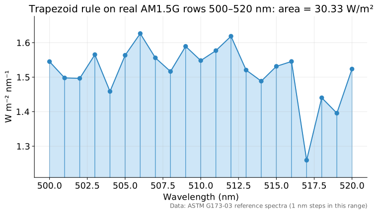
Spreadsheet recipe. Put wavelength in column A, AM1.5G in column C (rows 3–2004). In D4 enter =(C3+C4)/2*(A4-A3) and fill down. =SUM(D4:D2004) gives the total. For a band, sum only the rows inside it (use SUMIFS on column A).
Python recipe.
import numpy as np
d = np.genfromtxt("ASTMG173.csv", delimiter=",", skip_header=2)
wl, am0, g, dni = d.T
print(np.trapezoid(g, wl))            # ≈ 1000.4 W/m²
band = (wl >= 380) & (wl <= 750)
print(np.trapezoid(g[band], wl[band]) / np.trapezoid(g, wl))   # visible fraction ≈ 0.50
Reference results to check yourself against
Computed on this site from ASTM G173-03 with the trapezoid rule:
| Quantity | AM0 | AM1.5G | AM1.5D |
|---|---|---|---|
| Total, 280–4000 nm (W/m²) | 1347.9 | 1000.4 | 900.1 |
| UV share (< 400 nm) | 7.6 % | 4.6 % | 3.4 % |
| Visible share (380–750 nm) | 45.9 % | 50.4 % | 48.8 % |
| Beyond Si cutoff (> 1107 nm) | 24.8 % | 19.2 % | 20.7 % |
| Photon flux (s⁻¹ m⁻²) | 6.15 × 10²¹ | 4.31 × 10²¹ | 3.99 × 10²¹ |
From spectrum to maximum current
Convert each row to photon flux, \(\Phi_\lambda = E_\lambda \lambda/(hc)\), integrate up to the cutoff wavelength \(\lambda_g = 1239.84/E_g\), and multiply by \(q\):
In words: count every photon energetic enough to be absorbed and give each one electron.
| Band gap (eV) | Cutoff (nm) | \(J_{sc,\max}\) AM1.5G (mA/cm²) | "Ultimate" efficiency* |
|---|---|---|---|
| 0.67 (Ge) | 1851 | 61.1 | 40.9 % |
| 1.12 (Si) | 1107 | 43.8 | 49.0 % |
| 1.34 (SQ optimum) | 925 | 35.0 | 46.9 % |
| 1.42 (GaAs) | 873 | 32.0 | 45.5 % |
| 1.50 (CdTe) | 827 | 28.9 | 43.4 % |
| 1.60 (perovskite, typical) | 775 | 25.4 | 40.6 % |
| 1.75 (top cell for Si tandem) | 708 | 21.0 | 36.8 % |
*"Ultimate efficiency" = \(E_g \times\) (photon flux above \(E_g\)) ÷ incident power: every absorbed photon delivers exactly \(E_g\) of energy. It accounts for below-gap and thermalization losses only (Unit 11). All values computed here.
Worked example — the silicon number by hand (sanity check)
From the table, photon flux above 1.12 eV ≈ \(J/q = 437.7\ \text{A/m}^2 / 1.602\times10^{-19} = 2.73\times10^{21}\) s⁻¹m⁻². If each delivered 1.12 eV \(= 1.794\times10^{-19}\) J, power \(= 2.73\times10^{21} \times 1.794\times10^{-19} = 490\) W/m² → 49 % of 1000 W/m². ✔ matches the table.
Lab exercise (do this)
- Download the G173 table (or the pvlib CSV). Plot all three columns vs wavelength.
- Reproduce the "Reference results" table above to within 0.5 %.
- Compute \(J_{sc,\max}\) for band gaps from 0.6 to 2.4 eV in 0.05 eV steps and plot it. Where does it fall fastest, and why (look at the spectrum)?
- Compute the fraction of AM1.5G power between 300 and 1200 nm (roughly silicon's response range).
- Extension: multiply AM1.5G by a made-up quantum-efficiency curve (1.0 from 400–1000 nm, linear to 0 at 1200 nm and at 300 nm) and integrate to get a realistic \(J_{sc}\).
Expected: (4) ≈ 84 %; (5) with exactly that QE shape ≈ 42.4 mA/cm² (computed here) — higher than real cells (≈ 41–42 mA/cm²) because a real QE is below 1 everywhere due to reflection and metal shading. If your totals are off by 10–30 %, you probably assumed uniform spacing.
Common misconceptions
Misconceptions
- "Add up the column to get W/m²." Only if every step is exactly 1 nm. Multiply by the step width (trapezoid rule).
- "Power fraction = photon fraction." No. Photons are weighted toward the red: beyond 1107 nm lies 19 % of AM1.5G power but about 36 % of its photons (computed here).
- "Higher Jsc means a better band gap." Jsc rises as the gap falls, but voltage falls; the optimum balances both (Unit 11).
What this means for manufacturing and the job
- QE → Jsc integration is how labs cross-check flash-test currents (SOL 401).
- Spectral mismatch factor \(M\) is a ratio of four such integrals (test cell vs reference cell, simulator vs AM1.5G) used to calibrate production testers.
- Data handling: the job requirements emphasise Python/SQL data analysis on process data; this is a gentle first exercise with a real standard dataset.
Review questions
1. Why can't you just sum the G173 irradiance column?
Step sizes vary (0.5, 1 and 5 nm); each value must be multiplied by its step width (trapezoid rule).
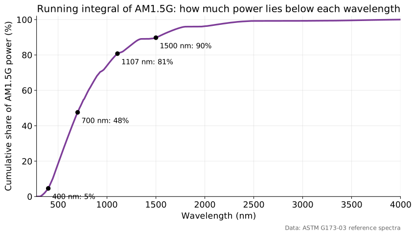
2. What is the AM1.5G power between 400 and 700 nm (use the cumulative figure)?
About 48 % − 5 % ≈ 43 % of 1000 W/m² ≈ 430 W/m².
3. Max Jsc for a 1.42 eV GaAs cell under AM1.5G?
≈ 32.0 mA/cm² (table).
4. Why is the 'ultimate efficiency' of Si (49 %) higher than its SQ limit (≈ 33 %)?
Ultimate efficiency counts only below-gap and thermalization losses; SQ also includes unavoidable radiative recombination, which keeps the voltage below \(E_g/q\) and the fill factor below 1.
5. Integrated AM1.5G photon flux is 4.31 × 10²¹ s⁻¹m⁻². If every photon gave one electron, what current density would that be?
\(q\Phi = 690\) A/m² = 69 mA/cm² — only reachable by a zero-gap absorber, which would give zero voltage.
Sources
- ASTM G173-03 data (pvlib-python copy,
pvlib/data/ASTMG173.csv, downloaded 3 Oct 2026). All integrals on this page computed by the author of this course with the trapezoid rule. - PVEducation, "Spectral Irradiance" and "Photon Flux" pages.