Unit 5 — Point Defects, Dislocations and Impurities in Silicon
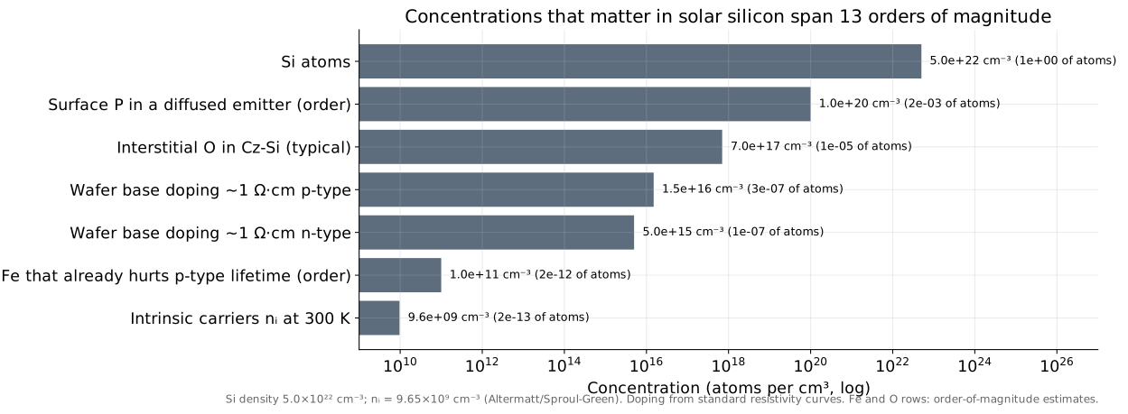
Big idea. No crystal is perfect. Missing atoms, extra atoms, foreign atoms and misaligned rows all exist. Some impurities are deliberate (dopants, at ~10¹⁵–10²⁰ cm⁻³); others — especially transition metals like iron at levels as low as ~10¹¹ cm⁻³ (a few parts per trillion) — destroy carrier lifetime. Oxygen from the quartz crucible and the boron–oxygen defect explain much of the industry's shift from p-type to n-type wafers.
Learning objectives
- Classify defects as point, line, planar or volume, with examples.
- Distinguish shallow (dopant) and deep (trap) levels in the band gap.
- Estimate a Shockley–Read–Hall lifetime from trap density.
- Explain the roles of Fe, Cu, O, C, B–O and gettering in solar silicon.
- Relate resistivity specs to doping concentration.
Why this matters
Carrier lifetime — how long a light-generated electron survives — is the material quality metric for cells; it is controlled by defects. Contamination control and cleanroom practice appear in 12 of 31 Tesla/SpaceX solar postings (see 01-job-requirements.md), and they exist because of this unit.
A taxonomy of defects
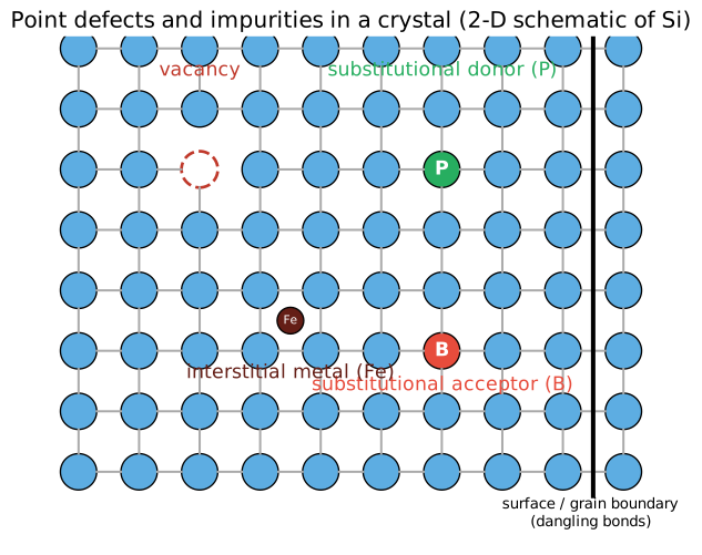
| Dimension | Defect | Examples in solar Si |
|---|---|---|
| 0-D (point) | vacancy, self-interstitial, substitutional or interstitial impurity, small complexes | V, I, P_Si, B_Si, Fe_i, FeB pairs, B–O complex |
| 1-D (line) | dislocations (edge, screw) | from thermal stress in crystal growth, cracks |
| 2-D (planar) | grain boundaries, twin boundaries, stacking faults, surfaces | multicrystalline wafers; wafer surfaces |
| 3-D (volume) | precipitates, voids | oxygen precipitates, metal silicides |
Shallow and deep levels
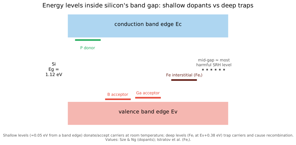
A substitutional phosphorus atom's fifth electron is bound by only ~0.045 eV — easily freed by thermal energy at room temperature (\(k_BT \approx 0.026\) eV). Its energy level lies just below the conduction band: a shallow donor. Boron's level lies ~0.045 eV above the valence band: a shallow acceptor. These set conductivity — that's doping.
Transition metals, vacancies and many complexes create deep levels near mid-gap. A deep level can capture an electron and then a hole (or vice versa), annihilating a pair: Shockley–Read–Hall (SRH) recombination. Mid-gap levels are the most efficient recombination centres.
Lifetime from trap density
For a trap density \(N_t\) with capture cross-section \(\sigma\) and carrier thermal velocity \(v_{th}\), the minority-carrier SRH lifetime (low injection, efficient trap) is approximately
In words: lifetime is the average time before a carrier bumps into a trap and is captured.
Worked example 1 — how little iron hurts
Take \(\sigma = 1\times10^{-14}\) cm² and \(v_{th} = 1\times10^{7}\) cm/s (round illustrative values; real \(\sigma\) depends on trap and carrier type). For \(N_t = 10^{12}\) cm⁻³ (that is 0.02 ppba!): \(\tau = 1/(10^{-14}\times10^{7}\times10^{12}) = 10^{-5}\) s = 10 µs. Diffusion length \(L = \sqrt{D\tau} = \sqrt{30 \times 10^{-5}} \approx 0.017\) cm = 170 µm for electrons (\(D \approx 30\) cm²/s, estimate). For high-efficiency cells we want ms lifetimes — trap densities below ~10¹⁰ cm⁻³.
Metals: the lifetime killers
Iron, copper, nickel, chromium, titanium and others enter from equipment, crucibles, chemicals and handling. They diffuse fast (Unit 7) and form deep levels or precipitates. Iron is the most studied: in boron-doped p-type silicon, interstitial Fe pairs with B (FeB), and light or heat splits the pairs — a measurable signature used to quantify iron. Importantly, interstitial Fe hurts p-type silicon (minority electrons) far more than n-type (minority holes) because of asymmetric capture cross-sections — one reason n-type wafers tolerate contamination better (Macdonald & Geerligs, 2004).
Gettering moves metals away from the active region: phosphorus diffusion gettering (metals segregate into the heavily doped P layer), boron-diffusion gettering, aluminium gettering, and hydrogenation (H from SiNₓ passivates residual defects). These are built into cell processes (SOL 302).
Oxygen and carbon
In Czochralski growth the silicon melt dissolves the silica crucible, so Cz wafers contain interstitial oxygen around 10¹⁷–10¹⁸ cm⁻³ (order of magnitude). Oxygen: - strengthens wafers against dislocation slip (good), - forms thermal donors when held around 350–500 °C (shifts resistivity), - forms oxygen precipitates and ring-shaped defect patterns after high-temperature steps (bad for lifetime — a known issue for n-type TOPCon wafers), - combines with substitutional boron into the B–O defect that causes light-induced degradation (LID) in boron-doped p-type cells (a few % relative power loss in the first days of sunlight, historically). The industry fixed it by gallium doping of p-type wafers and, more fundamentally, by moving to phosphorus-doped n-type wafers, which have no B–O defect (SOL 403).
Carbon (from graphite hot-zone parts and feedstock) is mainly harmful through its interaction with oxygen precipitation.
Dislocations
Dislocations are line defects — an extra half-plane of atoms (edge) or a helical shift (screw). They form when thermal stress during crystal growth or cooling exceeds the yield stress. They are recombination-active, especially when decorated with metals. A Cz ingot that develops dislocations "loses structure" and the affected part is typically remelted — a key yield metric (SOL 301).
Resistivity and doping
Wafers are specified by resistivity (Ω·cm) rather than doping concentration because it's easy to measure (four-point probe, SOL 401). Roughly (standard Irvin-type curves): 1 Ω·cm ≈ 5 × 10¹⁵ cm⁻³ phosphorus (n-type) or ≈ 1.5 × 10¹⁶ cm⁻³ boron (p-type) — p-type needs more dopant for the same resistivity because holes are less mobile than electrons.
Common misconceptions
Misconceptions
- "Nine-nines polysilicon means impurity effects are negligible." 9N still allows ~5 × 10¹³ impurity atoms/cm³ in total; specific metals must be far below that.
- "All impurities are bad." Dopants are essential; oxygen even helps mechanically.
- "Defects only matter at the surface." Bulk defects limit lifetime throughout the wafer; surfaces are handled by passivation.
- "LID is a module defect." It is a wafer-material effect (B–O), now largely engineered out.
What this means for manufacturing and the job
- Contamination control (metal-free tools, clean chemicals, gloves, wafer carriers) protects lifetime; SpaceX/Tesla postings repeatedly mention contamination and cleanroom practice.
- Lifetime measurement (QSSPC, µ-PCD, PL imaging) is standard incoming wafer QC and process monitoring (SOL 401).
- n-type transition and Ga-doped p-type were responses to B–O LID (SOL 301/403).
Review questions
1. Classify: vacancy, dislocation, grain boundary, oxygen precipitate.
0-D, 1-D, 2-D, 3-D.
2. Why does a mid-gap level recombine carriers more efficiently than a shallow level?
A mid-gap trap can capture both an electron (from the conduction band) and a hole (from the valence band) with comparable ease; a shallow level mostly exchanges carriers with its nearby band and re-emits them thermally.
3. With σ = 1 × 10⁻¹⁴ cm², v = 10⁷ cm/s, what trap density gives τ = 1 ms?
N = 1/(σ v τ) = 1/(10⁻¹⁴ × 10⁷ × 10⁻³) = 10¹⁰ cm⁻³.
4. Why does Cz silicon contain oxygen, and name one bad and one good effect.
The melt dissolves the silica crucible. Bad: B–O LID, thermal donors, precipitates. Good: pins dislocations, strengthening the wafer.
5. Why are n-type wafers more tolerant of iron?
Interstitial iron captures minority electrons much more strongly than minority holes; in n-type wafers the minority carriers are holes.
Sources
- Sze & Ng, Physics of Semiconductor Devices — dopant ionisation energies.
- Istratov, Hieslmair & Weber, "Iron and its complexes in silicon", Appl. Phys. A 69, 13 (1999).
- Macdonald & Geerligs, Appl. Phys. Lett. 85, 4061 (2004) — impurity tolerance of n- vs p-type Si.
- Schmidt & Bothe on B–O LID (e.g., Phys. Rev. B 69, 024107 (2004)).
- Altermatt et al., J. Appl. Phys. 93, 1598 (2003) — nᵢ = 9.65 × 10⁹ cm⁻³ (Sproul & Green value refined).
- PVEducation, "Recombination" and "Lifetime" pages; ITRPV 17 for n-type share.