Unit 4 — Real Materials: Single-Crystal, Polycrystalline and Amorphous
Big idea. The same element can be one perfect crystal, a patchwork of many crystals (grains) joined at grain boundaries, or a disordered amorphous network. For solar cells, order matters because boundaries and disorder create electronic defects. That is why the industry moved from multicrystalline to monocrystalline wafers, and why thin films need grain-boundary treatments.
Learning objectives
- Define single crystal, multicrystalline, polycrystalline, microcrystalline and amorphous.
- Explain what a grain boundary is and why it can recombine carriers.
- Compare characteristic grain sizes with carrier diffusion lengths.
- Explain where each form is used in PV today (mono wafers; thin-film poly; a-Si:H layers).
Why this matters
Wafer type was the defining technology choice of the last decade: multicrystalline (cast) silicon was cheaper, but monocrystalline Czochralski (Cz) wafers gave higher efficiency and texture better; mono now dominates (n-type Cz mono about 82 % of 2025 c-Si production per ITRPV 17). Meanwhile amorphous silicon reappeared as the 5–10 nm passivation layer of heterojunction (HJT) cells.
Degrees of order
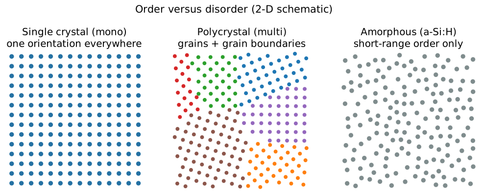
| Form | Grain size | How made | PV use |
|---|---|---|---|
| Monocrystalline (mono) | whole ingot (one crystal) | Czochralski pulling (Cz), float zone (FZ) | dominant wafer type today |
| Multicrystalline (mc) | mm – cm | directional solidification ("casting") | was majority until ~2018–2019; now marginal |
| Cast-mono / quasi-mono | large seeded grains | seeded casting | niche |
| Polycrystalline thin film | ~0.1 – few µm | vapour/solution deposition | CdTe, CIGS, perovskite |
| Microcrystalline Si (µc-Si:H) | ~10–100 nm crystallites in amorphous matrix | PECVD | historical tandem thin film; contact layers |
| Amorphous (a-Si:H) | none | PECVD from SiH₄ (+H₂) | HJT passivation; old thin-film modules |
(Dates and shares: ITRPV editions; treat as approximate.)
Grain boundaries
Where two grains meet, atoms cannot satisfy all their bonds: the boundary contains strained and dangling bonds whose energy levels lie in the band gap. These act as recombination centres (Unit 5) and also attract impurities (metals segregate to boundaries and dislocations, Unit 6). Boundaries can also bend the bands, creating barriers to current flow.
The key comparison: grain size vs diffusion length \(L\) (how far a carrier travels before recombining; SOL 201). If grains are much larger than \(L\) and than the wafer thickness, boundaries matter little; if grains are comparable to or smaller than \(L\), many carriers reach a boundary and recombine.
Worked example 1 — does grain size matter?
A good n-type mono wafer may have minority-carrier diffusion length > 1 mm (lifetime ~ ms; estimate) — far more than its 130 µm thickness. A multicrystalline wafer with mm-scale grains, lots of dislocations and decorated boundaries might have \(L\) of 100–300 µm in good grains but much less near boundaries (estimate). A CdTe film with 1 µm grains is only ~3 µm thick, so every carrier is within a micron or so of a boundary — which is why CdTe needs a CdCl₂ treatment to passivate boundaries (SOL 305).
Amorphous silicon
In a-Si, each atom still has roughly four neighbours, but bond angles and lengths vary randomly. Many dangling bonds remain; adding ~10 % hydrogen (a-Si:H, deposited by PECVD from silane) ties most of them off. Consequences:
- Band gap ≈ 1.7–1.8 eV (wider than c-Si), strong absorption (disorder relaxes momentum rules), but poor transport and light-induced degradation (Staebler–Wronski effect) — so a-Si thin-film modules were low efficiency.
- As an ultra-thin intrinsic layer (~5–10 nm) on crystalline silicon, a-Si:H gives superb surface passivation: the basis of HJT cells with very high \(V_{oc}\) (SOL 303). It must stay below ~200–250 °C after deposition or the hydrogen effuses — which forces low-temperature metallization (silver pastes cured at ~200 °C rather than fired).
Why mono won
- Fewer defects → higher lifetime and voltage.
- (100) orientation → alkaline pyramid texture (multi needs acid isotropic texture, which is less effective).
- Diamond-wire sawing + cheaper Cz (larger ingots, continuous recharging) erased mc's cost advantage.
- n-type compatibility: high-efficiency TOPCon/HJT/back-contact cells need high lifetime.
Common misconceptions
Misconceptions
- "Polycrystalline silicon is a cheaper kind of wafer." "Polysilicon" in industry usually means the feedstock (chunks from the Siemens process), not the wafer. Wafers are mono or multi.
- "Amorphous means no structure at all." Short-range order (near-neighbour bonding) remains.
- "Grain boundaries are always bad." In CdTe and perovskites, treated boundaries can be benign or even help separate charges; it's the electronic states that matter.
What this means for manufacturing and the job
- Crystal growth (Cz, SOL 301) aims for dislocation-free single crystals; "loss of structure" during pulling is a yield event engineers track.
- Wafer inspection (photoluminescence imaging, lifetime mapping) reveals grain boundaries and defect clusters (SOL 401).
- HJT lines manage the thermal budget of a-Si:H — a constraint you will see in SpaceX HJT postings (SOL 303).
Review questions
1. What is the difference between 'polysilicon' feedstock and a multicrystalline wafer?
Polysilicon is ultra-pure silicon chunks/rods from the Siemens/FBR process used to feed crystal growth; a multicrystalline wafer is sliced from a cast ingot with many grains.
2. Why does a grain boundary recombine carriers?
It contains dangling and strained bonds (and segregated impurities) whose states in the band gap capture electrons and holes.
3. Why can a-Si:H passivate c-Si surfaces even though a-Si:H itself is a poor absorber material?
Its hydrogen terminates dangling bonds at the c-Si surface, removing interface states; transport through a 5–10 nm layer is short enough.
4. Give two reasons mono replaced multi.
Higher lifetime/efficiency and alkaline texture on (100); cost reductions in Cz and diamond-wire sawing.
Sources
- ITRPV 17th ed. (2026) — wafer-type shares; earlier editions for the mc-to-mono transition.
- Green, Silicon Solar Cells; PVEducation "Multicrystalline Silicon" and "Amorphous Silicon" pages.
- Staebler & Wronski, Appl. Phys. Lett. 31, 292 (1977).
- Diffusion-length and grain-size figures marked as estimates.