Unit 11 — Preview: What Can Sunlight Do to a Semiconductor?
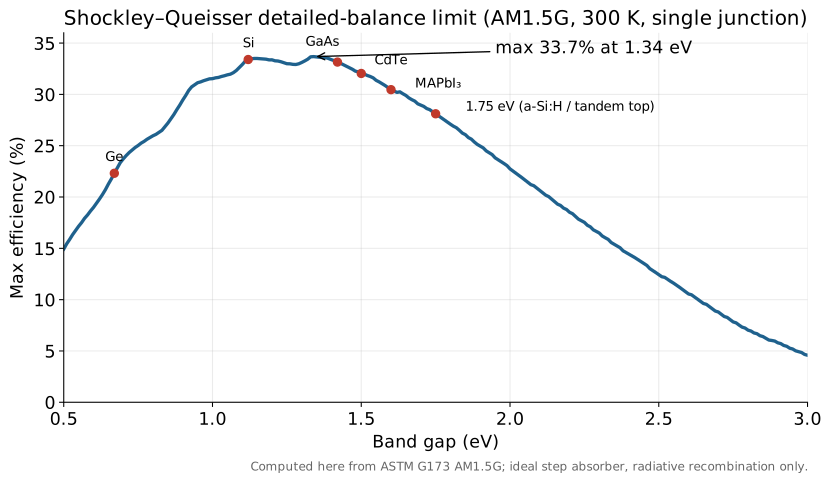
Big idea. A semiconductor has a band gap \(E_g\). Photons with less energy pass through; photons with more energy are absorbed, but their excess above \(E_g\) is lost as heat within picoseconds. A p-n junction sorts the freed electrons and holes to make a voltage and a current. Even a perfect cell loses energy to these effects and to unavoidable radiative recombination — the Shockley–Queisser limit, about 33.7 % at best and about 33.4 % for silicon. This unit previews SOL 201–203 and ties SOL 101 together.
Learning objectives
- Explain band gap, absorption, and thermalization with a band diagram.
- Describe in words how a p-n junction separates charge.
- Read an I–V and P–V curve: \(I_{sc}\), \(V_{oc}\), maximum power point, fill factor, efficiency.
- Compute the two "spectral" losses for silicon from the spectrum and state the SQ limit.
- Draw the first energy-loss waterfall from sunlight to an industrial cell.
Why this matters
This is the map for the whole curriculum. Every manufacturing step — texturing, doping, passivation, metallization, encapsulation — exists to remove one of the practical losses between the SQ limit and a real product. Job postings ask for "first-principles" understanding of cell performance; this waterfall is the first-principles picture.
Bands and band gaps
In an isolated atom, electrons occupy sharp energy levels. In a crystal of ~5 × 10²² atoms/cm³ those levels broaden into bands. In a semiconductor at low temperature, the valence band (bonding electrons) is full and the conduction band is empty, separated by a band gap \(E_g\) with no allowed states. Silicon: \(E_g = 1.12\) eV at 300 K.
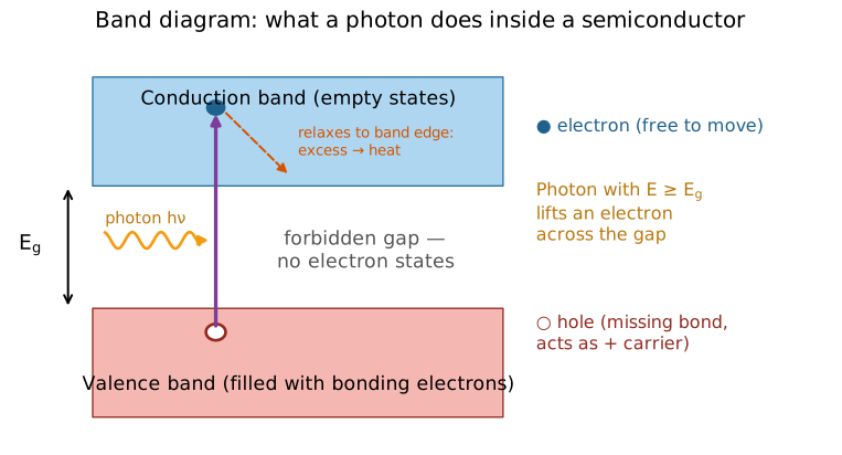
What happens to each photon:
| Photon energy | Outcome | Loss |
|---|---|---|
| \(E < E_g\) | not absorbed (transmitted, or absorbed by free carriers/back contact → heat) | below-gap loss: whole photon |
| \(E \ge E_g\) | creates one electron–hole pair | thermalization: \(E - E_g\) becomes heat |
The two spectral losses for silicon
Using the AM1.5G table (Unit 8) we can compute exactly how much power each loss takes for \(E_g = 1.12\) eV:
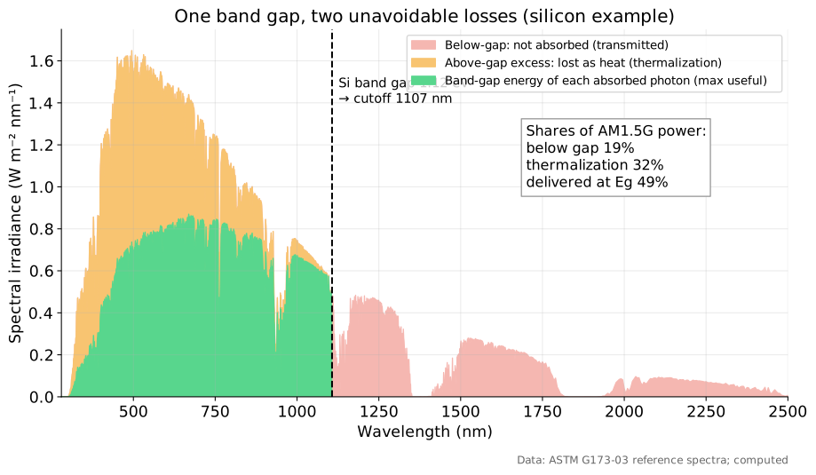
So even before any electrical physics, at most 49 % of sunlight's power can be delivered by a silicon absorber — the "ultimate efficiency" from Unit 8. Lower band gaps reduce the pink loss but increase the orange one; higher gaps do the opposite.
The p-n junction
Freeing electrons is not enough — they must be pushed in one direction. Doping silicon with phosphorus (5 valence electrons) makes it n-type (extra electrons); doping with boron (3 valence electrons) makes it p-type (extra holes). Where n and p regions meet, electrons and holes diffuse across and recombine, leaving fixed charged dopant ions that create a built-in electric field in a thin depletion region. Light-generated electrons are swept to the n side, holes to the p side: a voltage builds up, and connecting a load lets current flow.
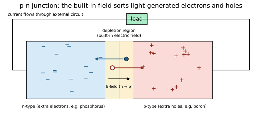
(How doping, Fermi levels and the junction work quantitatively is SOL 201–202.)
The I–V curve
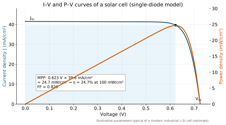
Sweep the voltage across an illuminated cell and record the current: the I–V curve. Key points:
- Short-circuit current \(I_{sc}\) (V = 0): set by photon collection.
- Open-circuit voltage \(V_{oc}\) (I = 0): set by how fast carriers recombine; always below \(E_g/q\).
- Maximum power point (MPP) \(V_{mp}, I_{mp}\): where \(P = VI\) is largest.
- Fill factor \(FF = \dfrac{V_{mp} I_{mp}}{V_{oc} I_{sc}}\): how "square" the curve is.
- Efficiency \(\eta = \dfrac{V_{oc} I_{sc} FF}{P_\text{in}}\).
Worked example 1 — reading the curve
\(J_{sc} = 41.5\) mA/cm², \(V_{oc} = 0.725\) V, MPP at 0.623 V and 39.6 mA/cm². \(P_{mp} = 0.623 \times 39.6 = 24.7\) mW/cm². \(FF = 24.7/(0.725 \times 41.5) = 0.82\). Efficiency \(= 24.7/100 = 24.7\) %. For a 330 cm² cell: \(P = 24.7 \times 330 = 8.1\) W at \(I_{mp} = 13.1\) A.
The Shockley–Queisser limit
In 1961 William Shockley and Hans Queisser asked: what is the best possible single-junction cell? Assume (1) every photon above \(E_g\) is absorbed and creates one electron–hole pair; (2) the only recombination is the unavoidable radiative kind required by detailed balance (a cell that absorbs must also emit, Unit 5); (3) the cell is at 300 K. Then the current is \(J = J_{sc} - J_0(e^{qV/k_BT} - 1)\), with \(J_0\) set by the cell's own blackbody emission above \(E_g\). Maximising \(V \times J\) for each gap gives the limit:
Worked example 2 — the SQ silicon cell
For \(E_g = 1.12\) eV our calculation gives \(J_{sc} = 43.8\) mA/cm², radiative \(J_0 \approx 8 \times 10^{-17}\) A/cm², and so \(V_{oc} = (k_BT/q)\ln(J_{sc}/J_0) = 0.02585 \times \ln(5.5 \times 10^{14}) \approx 0.88\) V — well below 1.12 V. The voltage deficit is the entropy cost of radiative emission (Unit 2). Efficiency at the MPP: 33.4 %.
Silicon is not at the SQ optimum (1.34 eV) — but it is only 0.3 percentage points below it, cheap, abundant, stable, non-toxic, and has 70 years of process know-how. That is why it dominates (≈ 98 % of production; ITRPV 17).
Beyond SQ for silicon: the real ceilings
- Auger recombination (three-particle process intrinsic to silicon) and silicon's weak, indirect absorption lower the realistic single-junction limit to 29.4 % (Richter, Hermle & Glunz, 2013; later refinements give similar values).
- Record cells are around 27–28 % (back-contact designs; check the Fraunhofer ISE Photovoltaics Report or NREL chart for the current figure).
- Industrial cells in mass production are about 25–26 % (TOPCon/HJT/back-contact; estimate consistent with ITRPV 17), and modules about 23.5–24 % (ITRPV 17).
The first energy-loss waterfall
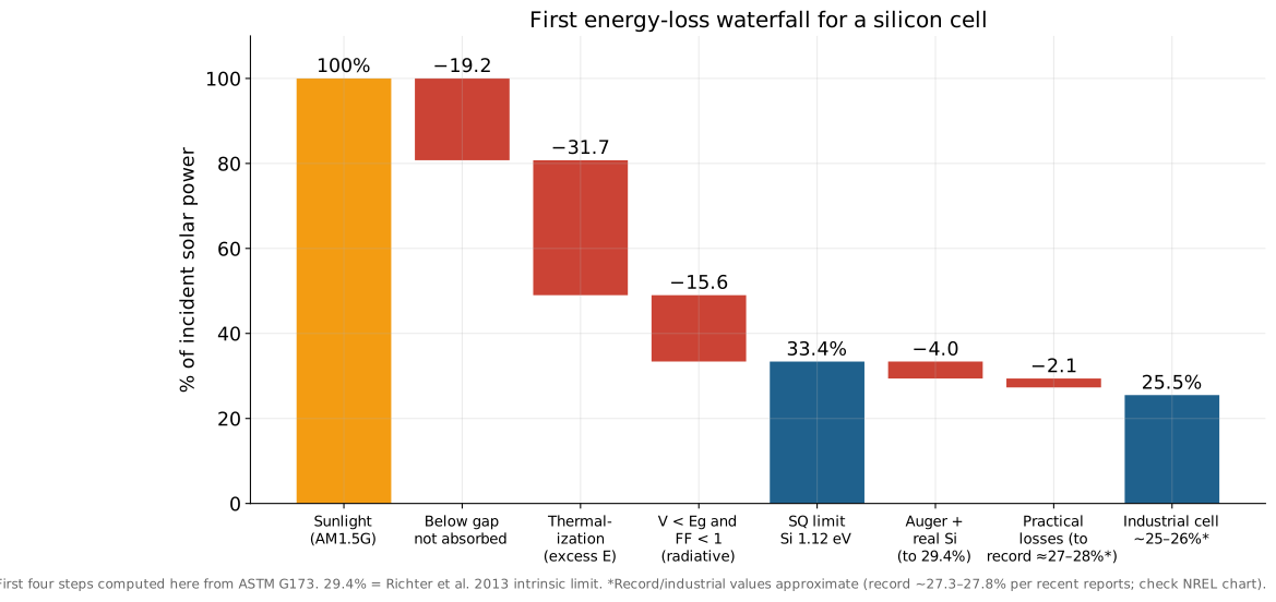
How to read it, left to right: 1. 100 % sunlight (AM1.5G). 2. −19 % below-gap photons (silicon cannot absorb beyond 1107 nm) → SOL 203 (tandems use them). 3. −32 % thermalization → also tandems; nothing else can recover it. 4. −16 % voltage and fill-factor penalty of an ideal radiative cell → thermodynamics (SOL 202/203). 5. = 33.4 % SQ limit for silicon. 6. −4 % Auger and other intrinsic silicon physics → 29.4 %. 7. −2 % practical losses in record cells (reflection, shading, resistance, surface/defect recombination). 8. ≈ 25.5 % industrial cells; then module losses down to ≈ 23.5 % (SOL 304).
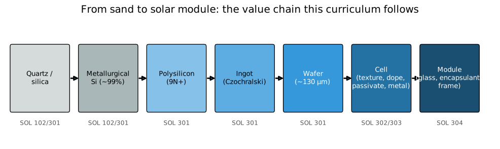
From sand to module: the road ahead
Common misconceptions
Misconceptions
- "A lower band gap is always better because it absorbs more light." It raises current but lowers voltage; the optimum is ~1.3–1.4 eV for one junction.
- "Voc equals the band gap." Even an ideal cell's \(V_{oc}\) is ~0.25–0.3 V below \(E_g/q\) at one sun.
- "The SQ limit is a materials problem that research will beat." It is a limit for one junction under unconcentrated sunlight; beating it requires changing the rules (tandems, concentration).
- "Silicon is used because it's the best absorber." It is a weak (indirect) absorber; it wins on abundance, stability, cost and manufacturing maturity.
What this means for manufacturing and the job
- Every process step maps to a loss: texture/ARC → reflection; passivation (Al₂O₃, SiNₓ, TOPCon poly-Si, HJT a-Si:H) → recombination and \(V_{oc}\); screen printing/metallization → shading and resistance (FF); module stack → optical and resistive losses.
- I–V metrics (\(J_{sc}\), \(V_{oc}\), FF, η) are the daily language of cell lines; process engineers trend them by tool and lot (SOL 401/402).
- Tandem readiness: ITRPV expects silicon-based tandems in mass production around 2027–2028; they attack the two biggest bars in this waterfall.
Key equations
| Equation | In words |
|---|---|
| \(\lambda_g = 1239.84/E_g\) | cutoff wavelength |
| \(FF = V_{mp}I_{mp}/(V_{oc}I_{sc})\) | squareness of the I–V curve |
| \(\eta = V_{oc}I_{sc}FF/P_\text{in}\) | efficiency from the three headline parameters |
| \(J = J_{sc} - J_0(e^{qV/k_BT}-1)\) | ideal diode under light |
| \(V_{oc} = (k_BT/q)\ln(J_{sc}/J_0 + 1)\) | open-circuit voltage |
Review questions
1. Which photons does a 1.5 eV CdTe cell not absorb?
Those with λ > 1239.84/1.5 ≈ 827 nm.
2. A 2.5 eV photon is absorbed by silicon. How much energy becomes heat (ideally)?
2.5 − 1.12 = 1.38 eV (55 % of the photon's energy).
3. Voc = 0.70 V, Jsc = 40 mA/cm², FF = 0.80. Efficiency at 100 mW/cm²?
0.70 × 40 × 0.80 = 22.4 mW/cm² → 22.4 %.
4. Why is the ideal Voc of silicon (≈ 0.88 V) lower than 1.12 V?
Because of unavoidable radiative recombination (detailed balance): the cell emits light, which at one sun limits the carrier build-up; the voltage deficit reflects the entropy of the emitted and absorbed radiation.
5. Name the two largest losses in the waterfall and the technology that addresses them.
Thermalization (≈ 32 %) and below-gap transmission (≈ 19 %); multi-junction (tandem) cells address both.
6. Why is the SQ optimum around 1.34 eV?
It balances current (more photons absorbed with lower gap) against voltage (higher with larger gap) for the AM1.5G spectrum.
Sources
- Shockley & Queisser, "Detailed Balance Limit of Efficiency of p-n Junction Solar Cells", J. Appl. Phys. 32, 510 (1961). SQ curve here recomputed from ASTM G173 AM1.5G at 300 K (results agree with the widely quoted 33.7 % at 1.34 eV).
- Richter, Hermle & Glunz, IEEE J. Photovoltaics 3, 1184 (2013).
- PVEducation, "Solar Cell Operation", "IV Curve", "Fill Factor", "Detailed Balance" pages.
- ITRPV 17th ed. (2026): production efficiencies, technology shares, tandem timeline. Fraunhofer ISE Photovoltaics Report (2026) for record efficiencies.