Unit 8 — The Chemistry of Silicon: Silica → Silicon, Chlorosilanes, Etching, Oxidation
Big idea. Silicon starts as silica (SiO₂) — sand and quartz. Carbon pulls the oxygen off in an electric arc furnace (98–99 % pure "metallurgical" silicon). Turning silicon into a volatile liquid (trichlorosilane), distilling it, and depositing it back as solid gives "nine-nines" polysilicon. On the cell line, chemistry continues: alkaline solutions etch pyramids, acid mixtures etch isotropically, HF strips oxides, and oxygen grows them.
Learning objectives
- Write and explain the carbothermic reduction of silica.
- Explain the Siemens process: hydrochlorination, distillation, CVD deposition; and the silane/FBR alternative.
- Explain anisotropic alkaline etching vs isotropic acid etching, with reactions.
- Describe thermal oxidation and the role of HF and RCA-type cleans.
- Identify the hazards that accompany each chemistry (preview of Unit 11).
Why this matters
Polysilicon is the most energy-intensive step in the PV value chain (SOL 301/404). Wet chemistry (texturing, cleaning, etching) is a large share of a cell line and is explicitly requested in SpaceX wet-process postings (01-job-requirements.md).
From quartz to metallurgical silicon
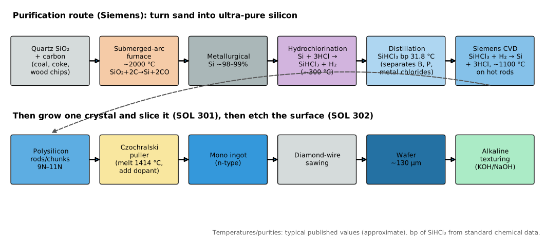
Silica's Si–O bonds are strong (Unit 2), so removing oxygen requires a powerful reducing agent and high temperature. In a submerged-arc furnace, quartz lumps and carbon (coal, coke, charcoal, wood chips) react at around 2000 °C, heated by graphite electrodes carrying huge currents:
(The real mechanism runs through intermediates such as SiO gas and SiC.) The product, metallurgical-grade silicon (MG-Si), is about 98–99 % Si, with Fe, Al, Ca, Ti, B and P impurities. Most MG-Si goes to aluminium alloys and silicones; a portion is refined for electronics and solar. Electricity use is commonly quoted around 11–13 kWh per kg (estimate; check SOL 301 sources).
The Siemens process
- Hydrochlorination / direct chlorination (fluidised bed, ~300 °C): \(\text{Si} + 3\,\text{HCl} \rightarrow \text{SiHCl}_3 + \text{H}_2\). Trichlorosilane (TCS) is a liquid boiling at 31.8 °C. Modern plants also convert the by-product SiCl₄ back to TCS by hydrogenation (\(3\,\text{SiCl}_4 + \text{Si} + 2\,\text{H}_2 \rightarrow 4\,\text{SiHCl}_3\)), closing the loop.
- Distillation: because impurities form chlorides with different boiling points (BCl₃, PCl₃, FeCl₃ …), fractional distillation purifies TCS to extreme levels.
- Deposition (CVD) in a bell-jar reactor: thin silicon "slim rods" are heated electrically to about 1100 °C in a TCS + H₂ atmosphere; \(\text{SiHCl}_3 + \text{H}_2 \rightarrow \text{Si} + 3\,\text{HCl}\). Over days the rods grow to ~15–20 cm diameter (estimate). They are then broken into chunks — polysilicon feedstock, solar grade typically 9N (99.9999999 %) or better; electronic grade 11N.
Alternative: silane + fluidised-bed reactor (FBR). TCS is converted to silane (SiH₄), which decomposes on small seed granules in a fluidised bed at lower temperature (~600–800 °C; estimate) to give granular polysilicon with lower energy use. Granular poly is increasingly used to top up continuous Cz pullers (SOL 301).
Worked example 1 — mass balance of the deposition reaction
\(\text{SiHCl}_3\) molar mass = 28.09 + 1.01 + 3 × 35.45 = 135.45 g/mol. Depositing 1 kg Si (35.6 mol) consumes at least 35.6 mol TCS = 4.82 kg of TCS and produces 107 mol HCl (3.9 kg) — in practice much more TCS passes through the reactor because per-pass conversion is incomplete, and by-products are recycled.
Alkaline (anisotropic) etching — pyramid texture
Hot dilute KOH or NaOH (a few %, ~80 °C, with additives) dissolves silicon:
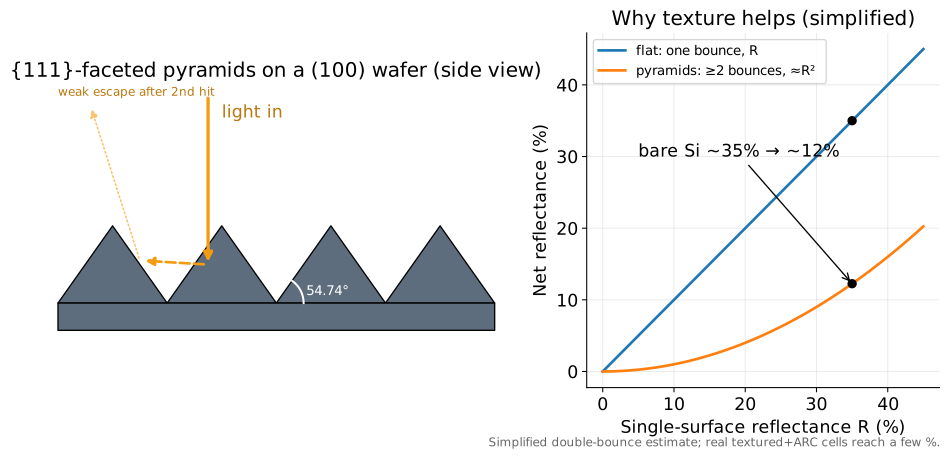
The etch rate on {111} planes is far lower than on {100} (Unit 3), so a (100) wafer develops random square-based pyramids with {111} faces at 54.74°, typically a few µm high. Light reflected from one facet usually strikes another, so reflection drops from ~35 % (flat) toward ~10–12 % before coating, and light enters the wafer at oblique angles (longer path → better absorption).
Historically isopropyl alcohol (IPA) was added to control pyramid nucleation; modern lines use proprietary additives instead, avoiding a flammable solvent in a hot bath.
Worked example 2 — hydrogen from texturing (a safety number)
Suppose texturing removes about 5 µm per side from a 182-mm wafer (assumption). Mass removed \(= 331\ \text{cm}^2 \times 2 \times 5\times10^{-4}\ \text{cm} \times 2.329\ \text{g/cm}^3 = 0.77\) g = 0.027 mol Si → 0.055 mol H₂ ≈ 1.2 L (at 0 °C, 1 atm) per wafer. A line texturing several thousand wafers an hour releases thousands of litres of hydrogen per hour — which is why wet benches have exhaust and are engineered for flammable gas.
Acid (isotropic) etching
A mixture of HNO₃ and HF etches silicon equally in all directions. Nitric acid oxidises the surface, HF dissolves the oxide:
Used for saw-damage removal, multicrystalline texturing (no preferred orientation needed), edge isolation and rear polishing. HF is exceptionally hazardous (Unit 11) — this chemistry is lecture-only in this curriculum.
Oxides: growing and stripping
Any silicon surface in air grows a native oxide ~1–2 nm thick. HF dissolves SiO₂ but not Si:
leaving a hydrogen-terminated, hydrophobic surface (water beads up — a classic process check). After POCl₃ diffusion, HF removes the phosphosilicate glass (PSG) layer.
Thermal oxidation grows SiO₂ deliberately: dry (\(\text{Si} + \text{O}_2 \rightarrow \text{SiO}_2\)) or wet/steam (\(\text{Si} + 2\,\text{H}_2\text{O} \rightarrow \text{SiO}_2 + 2\,\text{H}_2\)), at ~800–1100 °C. Growth is linear at first (reaction-limited) then parabolic (oxygen must diffuse through the growing oxide) — the Deal–Grove model. Each nanometre of oxide consumes about 0.44 nm of silicon. TOPCon cells use an ultra-thin (~1–2 nm) tunnel oxide under doped poly-Si; PERC/TOPCon rear stacks use oxides and Al₂O₃ for passivation.
Cleaning chemistry
The semiconductor industry's RCA clean (Kern, 1970) uses SC-1 (NH₄OH + H₂O₂ + H₂O; removes organics and particles) and SC-2 (HCl + H₂O₂ + H₂O; removes metals), often with HF dips. Solar lines use cheaper variants (e.g., ozone-based or HCl/HF cleans) tuned for cost and throughput. Purpose: remove metals before furnaces (Unit 7).
Common misconceptions
Misconceptions
- "Solar silicon is made by melting sand." Sand must be chemically reduced (oxygen removed) — melting doesn't do it.
- "Polysilicon is purified by melting." Chemical distillation of chlorosilanes does the heavy purification; crystal growth adds a final segregation step.
- "KOH just cleans the wafer." It sculpts it — removing microns of silicon to create texture.
- "HF is just a strong acid." It's a weak acid chemically, but uniquely toxic: it penetrates skin and binds calcium (Unit 11).
What this means for manufacturing and the job
- Polysilicon plants dominate energy and cost of the silicon chain (SOL 301/404).
- Wet benches (texture, clean, etch, PSG removal) are a core area for process technicians and engineers; bath chemistry, temperature, lifetime (number of wafers per bath) and replenishment are daily control items (SOL 302/402).
- Exhaust/H₂ management and HF safety are mandatory competencies (Unit 11).
Review questions
1. Write the overall carbothermic reduction and name its product grade.
SiO₂ + 2C → Si + 2CO; metallurgical-grade silicon (~98–99 %).
2. Why convert silicon into trichlorosilane before purifying it?
TCS is a volatile liquid (bp 31.8 °C) that can be purified by fractional distillation, separating impurity chlorides by boiling point — far more effective than purifying solid silicon.
3. Why does KOH produce pyramids on (100) wafers but not on multicrystalline wafers?
Its etch rate is orientation-dependent ({111} slow). On a (100) wafer this exposes {111} facets as pyramids; on mc-Si, grains have random orientations, so texture is non-uniform — acid isotropic texturing is used instead.
4. How much silicon is consumed growing 100 nm of thermal oxide?
≈ 0.44 × 100 = 44 nm.
5. What does a hydrophobic surface after an HF dip tell you?
The oxide has been fully removed, leaving a hydrogen-terminated silicon surface.
Sources
- Bernreuter Research, polysilicon production routes (Siemens vs FBR) — consulted in the curriculum research.
- Green, Silicon Solar Cells; PVEducation "Refining Silicon", "Texturing" pages.
- Seidel et al., J. Electrochem. Soc. 137, 3612 (1990) — KOH anisotropic etching.
- Deal & Grove, J. Appl. Phys. 36, 3770 (1965) — oxidation kinetics; Si consumption ratio from Sze/Plummer.
- Kern & Puotinen, RCA Review 31, 187 (1970) — RCA clean.
- Energy for MG-Si: commonly quoted range, marked estimate.