Unit 9 — Thin-Film Growth and Deposition Methods
Big idea. Modern cells are stacks of films only nanometres thick: silicon nitride anti-reflection layers (~75 nm), aluminium-oxide passivation (a few nm), tunnel oxides (~1.5 nm), doped poly-Si (~100 nm), a-Si:H (~5–10 nm), transparent conductive oxides (~70–100 nm). How a film nucleates and grows — and which deposition tool makes it — decides its optical, electrical and passivation quality.
Learning objectives
- Explain nucleation and the three classical growth modes.
- Describe the principles, temperatures and typical uses of CVD/PECVD/LPCVD, sputtering, evaporation, ALD and solution coating.
- Calculate vacuum mean free path and explain why deposition happens in vacuum.
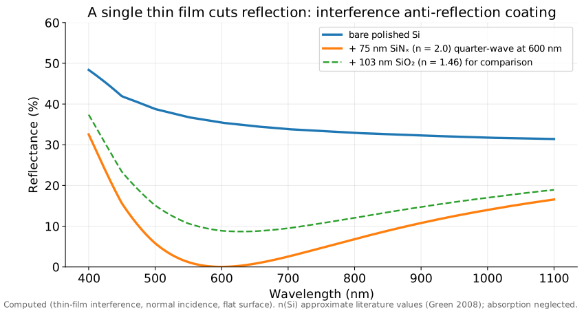
- Design a quarter-wave anti-reflection coating and explain the result with the reflectance figure.
- Estimate ALD cycle counts and thermal stress in films.
Why this matters
Thin-film deposition — PECVD, PVD/sputtering, ALD, CVD and TCOs — appears in 9 of 31 Tesla/SpaceX solar postings; vacuum/plasma systems in 5 (01-job-requirements.md). TOPCon, HJT and perovskite-on-silicon tandems are, physically, thin-film stacks on a wafer.
Nucleation
Atoms or molecules arriving at a surface (adatoms) diffuse around until they meet others and form clusters. Small clusters are unstable (too much surface energy for their volume) and fall apart; above a critical nucleus size they grow. Nucleation is easier on defects, steps and impurities (heterogeneous nucleation) than in free space. Higher substrate temperature lets adatoms diffuse further — fewer, larger grains; higher arrival rate gives more, smaller nuclei. The same ideas govern crystallisation from solution (Lab 102-A) and perovskite film formation.
Growth modes
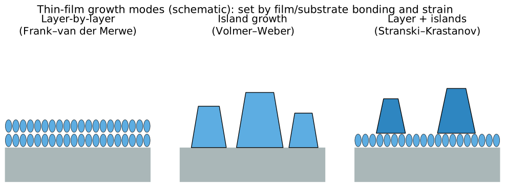
Which mode occurs depends on surface and interface energies (does the film "wet" the substrate?) and lattice mismatch. Most production films on solar cells are amorphous or polycrystalline and grow far from equilibrium, but the vocabulary is used in process discussions.
Why vacuum?
Many methods need low pressure so atoms travel from source to substrate without colliding with gas, and to keep films clean. The mean free path of a gas molecule is
Worked example 1 — mean free path
Nitrogen (\(d \approx 0.37\) nm), 300 K, \(p = 1\) Pa (0.0075 torr): \(\lambda = \dfrac{1.38\times10^{-23}\times300}{1.414\times\pi\times(3.7\times10^{-10})^2\times1} \approx 6.8\) mm. At atmospheric pressure (10⁵ Pa) it is ~68 nm; at 10⁻³ Pa (high vacuum) ~7 m — longer than the chamber, so evaporated atoms fly straight.
Deposition methods
| Method | How it works | Typical solar uses |
|---|---|---|
| Thermal CVD / APCVD / LPCVD | gases react on a hot substrate | LPCVD intrinsic/doped poly-Si for TOPCon (~600 °C); oxides |
| PECVD (plasma-enhanced CVD) | a plasma breaks up precursor gases (SiH₄, NH₃, N₂O, H₂…) so films form at 150–450 °C | SiNₓ:H ARC/passivation; a-Si:H for HJT; doped poly-Si precursor layers |
| ALD (atomic layer deposition) | alternating, self-limiting surface reactions — one sub-nm layer per cycle | Al₂O₃ passivation (TMA + H₂O/O₃), ~0.1 nm/cycle |
| Sputtering (PVD) | plasma ions knock atoms off a target onto the substrate | ITO/TCO for HJT and tandems; metal seed layers; CdTe-line TCOs |
| Evaporation (thermal/e-beam) | heat a source in high vacuum; vapour condenses on substrate | metal contacts in labs; some perovskite layers |
| Solution processing | spin-, blade-, slot-die- or spray-coating of precursor inks, then anneal | perovskites, some transport layers |
| Vapour transport / CSS | sublime a source onto a nearby hot substrate | CdTe (First Solar uses a vapour-transport process) |
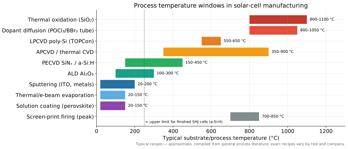
PECVD SiNₓ is the workhorse: silane and ammonia in a plasma at ~400 °C deposit hydrogen-rich silicon nitride; tuning gas ratios sets the refractive index (~1.9–2.3) and hydrogen content. ALD Al₂O₃ gives a few nm of film with negative fixed charge for passivating p⁺ surfaces; because each cycle self-limits, thickness is controlled by counting cycles, and coverage of textured surfaces is excellent. Industry uses spatial ALD or fast batch ALD for throughput.
Worked example 2 — ALD cycles
Target 6 nm Al₂O₃ at a growth per cycle of about 0.11 nm (typical literature value for TMA/H₂O; estimate): \(6/0.11 \approx 55\) cycles.
Designing an anti-reflection coating
A single transparent film of index \(n_1\) and thickness \(d\) on silicon cancels reflection at wavelength \(\lambda_0\) when it is a quarter-wave thick inside the film, and cancels it completely if its index is the geometric mean of the media on either side:
In words: the reflections from the top and bottom of the film travel half a wavelength apart and cancel; they cancel fully when both reflections are equally strong.
Worked example 3 — SiNₓ coating
In air (\(n_0 = 1\)) with \(n_\text{Si} \approx 3.94\) at 600 nm: ideal \(n_1 = \sqrt{3.94} = 1.98\) — silicon nitride! Thickness for \(\lambda_0 = 600\) nm: \(d = 600/(4\times2.0) = 75\) nm. Under glass/EVA (\(n_0 \approx 1.5\)), the ideal index rises to \(\sqrt{1.5\times3.94} \approx 2.4\), which is one reason module-optimised cells use slightly higher-index or graded SiNₓ stacks.
Stress and adhesion
Films deposited hot and cooled down are stressed if their thermal expansion differs from silicon's (Unit 10):
Large stress causes cracking, delamination or wafer bow. Intrinsic stress from the growth process (ion bombardment in sputtering, hydrogen content in PECVD) adds to it. Adhesion depends on interface chemistry and cleanliness — another reason for pre-deposition cleaning.
Common misconceptions
Misconceptions
- "Thicker coating = less reflection." Optical coatings work by interference at a specific thickness; too thick or too thin is worse.
- "Plasma is just for heating." The plasma supplies reactive radicals and ions so chemistry happens at low temperature.
- "ALD is too slow for factories." Spatial and batch ALD tools are used in high-volume PV lines.
- "Vacuum is only to keep films clean." It also lets atoms travel in straight lines and lets plasmas exist at useful conditions.
What this means for manufacturing and the job
- PECVD, ALD, sputter and LPCVD tools are the equipment backbone of TOPCon and HJT lines; engineers own film thickness/index uniformity, deposition rate, chamber cleaning (often with NF₃ — a hazardous, potent greenhouse gas; Unit 11) and uptime (SOL 302/303/402).
- Ellipsometry and reflectance measure film thickness and index daily (SOL 401).
- Vacuum skills (pumps, leak checks, plasma basics) are listed in postings (SOL 402 + Lab 402-B).
Review questions
1. Quarter-wave thickness of an n = 2.05 SiNₓ film for 620 nm?
620/(4 × 2.05) = 75.6 nm.
2. Why does PECVD let SiNₓ deposit at ~400 °C instead of ~800 °C?
The plasma dissociates SiH₄ and NH₃ into reactive radicals, supplying the energy that would otherwise come from heat.
3. Why is ALD good for textured wafers?
Self-limiting surface reactions coat every exposed surface uniformly (conformal), independent of line-of-sight.
4. Mean free path at 0.01 Pa (N₂, 300 K)?
6.8 mm × (1/0.01) = 0.68 m.
5. Ideal single-layer ARC index for silicon under EVA (n = 1.48)?
√(1.48 × 3.94) ≈ 2.41.
Sources
- Ohring, Materials Science of Thin Films; Smith, Thin-Film Deposition.
- PVEducation, "Anti-Reflection Coatings" page; Hecht, Optics (thin-film interference).
- Green, Sol. Energy Mater. Sol. Cells 92, 1305 (2008) — Si optical constants (approximate values used).
- George, "Atomic Layer Deposition: An Overview", Chem. Rev. 110, 111 (2010) — ALD growth per cycle.
- Temperature windows: compiled typical ranges (approximate).