Unit 12 — Computational Lab: Crystals, Phase Diagrams and Defect Numbers
Big idea. Doing the numbers yourself makes the course stick. In this lab you build a silicon crystal in Python and measure it, apply the lever rule and Scheil equation to realistic problems, estimate how many defects a crystal holds at high temperature, and convert between ppm, resistivity and atoms per cm³. Everything uses standard Python (numpy, matplotlib) — no special software.
Learning objectives
- Generate diamond-cubic coordinates and verify density, coordination and bond angle numerically.
- Predict XRD peak positions for silicon.
- Solve lever-rule and Scheil problems and plot ingot doping profiles.
- Estimate equilibrium vacancy concentrations and explain "frozen-in" defects.
- Fluently convert concentrations (ppma, ppba, cm⁻³) and resistivity.
Why this matters
Process engineers routinely script quick calculations: checking a supplier's resistivity spread, estimating contamination budgets, sanity-checking a metrology result. Postings ask for Python/data skills on top of materials knowledge; this lab joins the two.
Setup
Install Python 3 and run pip install numpy matplotlib. (On a Mac: python3 -m pip install --user numpy matplotlib.) Save each block as a .py file or paste into a Jupyter notebook.
Exercise 1 — build silicon
import numpy as np
a = 5.431  # Å
fcc = np.array([[0,0,0],[0,.5,.5],[.5,0,.5],[.5,.5,0]])
basis = np.vstack([fcc, fcc + 0.25])          # 8 atoms per cubic cell
cells = np.array([[i,j,k] for i in range(3) for j in range(3) for k in range(3)])
atoms = (basis[None,:,:] + cells[:,None,:]).reshape(-1,3) * a   # 3x3x3 supercell

# nearest neighbours of an interior atom
c = atoms[np.argmin(np.linalg.norm(atoms - 1.5*a - 0.25*a, axis=1))]
d = np.linalg.norm(atoms - c, axis=1)
nn = atoms[(d > 0.1) & (d < 2.5)]
print("neighbours:", len(nn), "distance:", d[(d>0.1)&(d<2.5)].round(3))
v = nn - c
cosang = v[0] @ v[1] / (np.linalg.norm(v[0]) * np.linalg.norm(v[1]))
print("bond angle:", np.degrees(np.arccos(cosang)).round(2))
print("atom density (cm^-3):", 8 / (a*1e-8)**3)
print("density (g/cm3):", 8*28.0855/6.02214e23/(a*1e-8)**3)mpl_toolkits.mplot3d to reproduce the Unit 3 figure.
Exercise 2 — XRD peaks
For diamond cubic, allowed reflections have \(h, k, l\) all odd, or all even with \(h+k+l\) divisible by 4. Compute \(2\theta\) for Cu Kα (1.5406 Å):
import itertools, numpy as np
lam, a = 1.5406, 5.431
peaks = set()
for h,k,l in itertools.product(range(5), repeat=3):
    if (h,k,l) == (0,0,0): continue
    odd = h%2 and k%2 and l%2
    even = (h%2==0 and k%2==0 and l%2==0 and (h+k+l)%4==0)
    if not (odd or even): continue
    d = a/np.sqrt(h*h+k*k+l*l); s = lam/(2*d)
    if s < 1: peaks.add((round(2*np.degrees(np.arcsin(s)),2), tuple(sorted((h,k,l), reverse=True))))
for p in sorted(peaks)[:5]: print(p)Exercise 3 — lever rule and Scheil
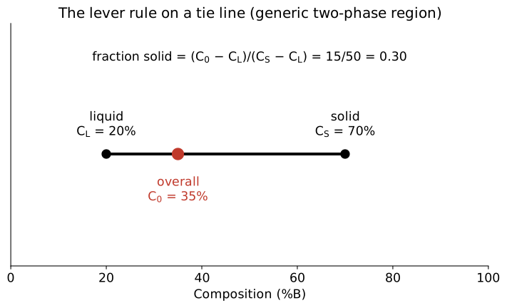
import numpy as np, matplotlib.pyplot as plt
fs = np.linspace(0, 0.95, 200)
for k, name in [(0.35,"P"), (0.8,"B"), (0.008,"Ga")]:
    plt.plot(fs, (1-fs)**(k-1), label=name)   # C_s relative to seed end
plt.yscale("log"); plt.xlabel("fraction solidified"); plt.ylabel("doping / seed-end doping"); plt.legend(); plt.show()Exercise 4 — vacancies and frozen-in defects
Equilibrium vacancy concentration follows \(n_v \approx N \exp(-E_f/k_BT)\) (ignoring the entropy prefactor). The formation energy \(E_f\) of a vacancy in Si is uncertain in the literature (roughly 3–4+ eV).
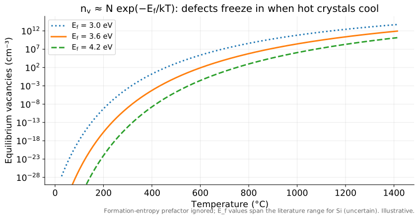
Compute \(n_v\) at 1400 °C and 25 °C for \(E_f = 3.6\) eV. (Answer: ≈ 7 × 10¹¹ cm⁻³ and ≈ 10⁻³⁸ cm⁻³ — i.e., none.)
Exercise 5 — concentration conversions
Fill in this table (Si atom density 5.0 × 10²² cm⁻³):
| Quantity | cm⁻³ | ppma |
|---|---|---|
| 1 ppma | ? | 1 |
| n-type base, 1 Ω·cm | ≈ 5 × 10¹⁵ | ? |
| Fe that measurably hurts p-type lifetime | ≈ 10¹¹ | ? |
| Interstitial O in Cz | ≈ 7 × 10¹⁷ | ? |
(Answers: 5 × 10¹⁶; 0.1 ppma; 2 × 10⁻⁶ ppma = 2 ppta; 14 ppma.)
Exercise 6 — an SRH budget
Using \(\tau = 1/(\sigma v_{th} N_t)\) with \(\sigma = 10^{-14}\) cm², \(v_{th} = 10^7\) cm/s, find the trap density allowed for \(\tau\) = 100 µs, 1 ms and 5 ms, and express each in ppta. (Answers: 10¹¹, 10¹⁰, 2 × 10⁹ cm⁻³ → 2, 0.2, 0.04 ppta.) This is why high-efficiency n-type lines obsess over metal contamination.
Deliverables
Save your scripts and a one-page summary with: the density/coordination check, the XRD peak list, the two ingot in-spec fractions, the vacancy plot and the conversion table. Keep them — SOL 201 and SOL 301 reuse them.
Review questions
1. Why are (100) and (110) reflections absent in the diamond-cubic XRD pattern?
The structure factor of the diamond basis makes them cancel: for diamond cubic, reflections occur only for all-odd hkl or all-even hkl with h+k+l divisible by 4.
2. Why does Ga-doped p-type silicon have a lower in-spec ingot fraction than P-doped n-type for the same resistivity window?
Ga's segregation coefficient (0.008) is far below P's (0.35), so its concentration rises much faster along the ingot.
3. Explain 'frozen-in' vacancies.
At high temperature many vacancies exist in equilibrium; on cooling they cannot all diffuse out in time, so excess vacancies remain and agglomerate into voids or complexes.
4. Convert 0.5 ppba to cm⁻³.
0.5 × 10⁻⁹ × 5 × 10²² = 2.5 × 10¹³ cm⁻³.
Sources
- Kittel (structure factor of diamond); Cullity & Stock, Elements of X-Ray Diffraction.
- Silicon XRD reference peaks: standard powder-diffraction data (e.g., NIST SRM 640 silicon).
- Scheil: Unit 6 sources. Vacancy formation energies: literature range (uncertain; illustrative).