Unit 2 — Chemical Bonding: Covalent, Ionic, Metallic
Big idea. Atoms bond by sharing or transferring valence electrons. The type of bond — covalent, ionic or metallic — decides whether a material is a semiconductor, an insulator or a conductor; whether it is hard or soft, brittle or ductile; and how strongly it absorbs light. Silicon is a covalent network solid; silver is metallic; glass is a mixed covalent-ionic network; halide perovskites are strongly ionic.
Learning objectives
- Distinguish covalent, ionic, metallic and weak (van der Waals, hydrogen) bonds.
- Use electronegativity difference to predict bond character.
- Explain sp³ hybridisation and the tetrahedral bonding of silicon.
- Connect bond strength and bond character to band gap, melting point, hardness and conductivity.
- Explain hydrogen passivation of dangling bonds.
Why this matters
"Why silicon? Why CdTe? Why does hydrogen in SiNₓ improve cells? Why do silver contacts conduct and glass not?" — all are bonding questions. Passivation, the main lever on cell voltage, is bond chemistry at surfaces.
Covalent bonds
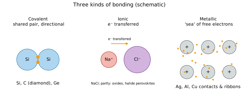
In a covalent bond two atoms share a pair of electrons. Silicon mixes its one 3s and three 3p orbitals into four equivalent sp³ hybrid orbitals pointing to the corners of a tetrahedron, 109.47° apart. Each overlaps with a neighbour's orbital to form a shared-pair bond. Every Si atom bonds to exactly four neighbours — a rigid, directional 3-D network.
Consequences: high melting point (1414 °C), hardness, brittleness (bonds can't slide; they break — wafers crack rather than bend), and a band gap: electrons are locked in bonds unless given at least \(E_g\) (1.12 eV) to break free.
Ionic bonds
When one atom pulls much harder than the other, an electron is effectively transferred: Na gives one to Cl, making Na⁺ and Cl⁻ that attract electrostatically in all directions. Ionic solids are brittle, have high melting points, are usually insulating with large band gaps, and often dissolve in water.
Metallic bonds
In metals, valence electrons are not tied to any atom; they form an electron "sea" around positive ion cores. Free electrons make metals excellent conductors and reflect light (shiny); non-directional bonding lets planes of atoms slide, so metals are ductile — copper ribbon bends, silicon snaps. Room-temperature resistivities (standard values): Ag 1.59, Cu 1.68, Al 2.65 µΩ·cm. Silver is the best conductor of all — and its cost and supply are why the industry works hard to reduce silver per cell (ITRPV).
Electronegativity and bond character
Real bonds lie on a spectrum. The electronegativity difference ΔEN predicts where:
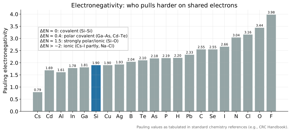
| Bond | ΔEN | Character | Where in PV |
|---|---|---|---|
| Si–Si | 0 | covalent | absorber |
| Ga–As | 0.37 | polar covalent | III–V cells |
| Cd–Te | 0.41 | polar covalent | CdTe thin film |
| Si–H | 0.30 | covalent | passivation (a-Si:H, SiNₓ:H) |
| Si–N | 1.14 | polar covalent | SiNₓ anti-reflection/passivation |
| Si–O | 1.54 | strongly polar | SiO₂, glass, native oxide |
| Pb–I | 0.33 (but ionic lattice) | ionic-covalent | halide perovskites |
(Perovskite bonding is better described as ionic overall, despite modest Pauling differences; it explains their soft lattice and low-temperature processing — SOL 305.)
Bond strength and the band gap
Stronger, shorter bonds put the bonding (valence) states further below the antibonding (conduction) states, so the band gap grows:
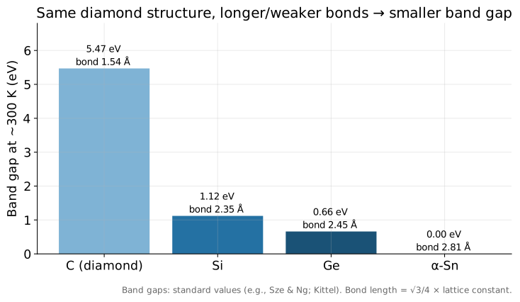
Adding ionic character at the same bond length widens the gap: Ge (0.66 eV), GaAs (1.42 eV) and ZnSe (≈ 2.7 eV) all sit in the same row with similar lattice constants. This is the logic of band-gap engineering in III–V and II–VI compounds (SOL 305).
Typical average bond energies (tabulated values, approximate): Si–Si ≈ 2.3 eV (≈ 222 kJ/mol), Si–H ≈ 3.3 eV, Si–O ≈ 4.7 eV. The Si–O bond is much stronger than Si–Si — which is why reducing sand to silicon costs so much energy (Unit 8) and why a native oxide forms instantly on any silicon surface exposed to air.
Dangling bonds and hydrogen passivation
At a surface or grain boundary, silicon atoms are missing neighbours: they have dangling bonds — half-filled orbitals with energies inside the band gap. These trap electrons and holes and make them recombine (Unit 5; SOL 201), killing voltage. Passivation ties them off:
- Chemical passivation: bond hydrogen (Si–H), oxygen (SiO₂) or a matched layer (a-Si:H, poly-Si/SiOₓ) to the dangling bonds, removing their states from the gap.
- Field-effect passivation: fixed charge in a coating (negative in Al₂O₃, positive in SiNₓ) repels one carrier type from the surface so recombination needs partners that aren't there.
Hydrogen-rich SiNₓ deposited by PECVD releases hydrogen during firing, which diffuses into the wafer and passivates defects in the bulk too.
Weak bonds
Van der Waals forces (fluctuating dipoles) and hydrogen bonds are 10–100× weaker than covalent bonds but govern polymers: they hold EVA and POE chains together, set their softness and glass-transition temperature, and control adhesion between encapsulant and glass (often aided by silane coupling agents that make covalent links — Unit 10).
Common misconceptions
Misconceptions
- "Bonds are either ionic or covalent." It's a continuum; most PV materials are mixed.
- "A stronger material conducts better." Strong covalent bonds lock electrons in place — diamond is an insulator.
- "Passivation is a protective coating like paint." It is electronic: it removes or neutralises recombination states at the atomic scale.
- "Metals are good contacts to silicon automatically." Metal–semiconductor contacts need careful engineering (doping, alloying, fire-through) to be low-resistance and low-recombination (SOL 302).
What this means for manufacturing and the job
- Passivation layers (Al₂O₃ by ALD, SiNₓ:H by PECVD, a-Si:H for HJT, SiOₓ/poly-Si for TOPCon) are the core of modern cell architectures (SOL 302/303).
- Wafer brittleness drives breakage-yield engineering in handling and stringing (SOL 402).
- Metallization choices (Ag, Cu plating, Ag-coated Cu) balance conductivity, cost and contact chemistry (SOL 302).
Review questions
1. Predict the bond type for Al–O (ΔEN = 1.83).
Strongly polar to ionic — Al₂O₃ is an ionic-covalent insulating ceramic.
2. Why are silicon wafers brittle while copper ribbons are ductile?
Directional covalent bonds in Si cannot slide; metallic bonding is non-directional, letting atomic planes glide (dislocation motion).
3. Explain why GaAs has a larger band gap than Ge despite similar lattice constants.
Ga–As bonds are partly ionic; ionic character separates bonding and antibonding energies further, widening the gap.
4. What is a dangling bond and why is it harmful?
An unsatisfied bonding orbital at a surface/defect; it creates states in the gap that capture carriers and cause recombination, lowering lifetime and voltage.
5. Name one chemical-passivation and one field-effect-passivation mechanism.
Chemical: hydrogen bonding to dangling bonds (Si–H). Field-effect: negative fixed charge in Al₂O₃ repelling electrons from a p-type surface.
Sources
- Callister & Rethwisch, Materials Science and Engineering, ch. 2 (bonding).
- Pauling electronegativities and resistivities: CRC Handbook. Bond energies: typical tabulated averages (e.g., general chemistry texts) — approximate.
- Sze & Ng, Physics of Semiconductor Devices; Kittel — band gaps.
- PVEducation, "Surface Recombination" and "Passivation" pages; ITRPV 17 on silver reduction.