Unit 1 — Atoms, Electrons and the Periodic Table
Big idea. A material's behaviour is decided by its outermost (valence) electrons. Silicon has four, which lets every atom bond to four neighbours — the root of its crystal structure and semiconducting behaviour. Elements one column to the left (boron, gallium) or right (phosphorus) of silicon are the dopants that make solar cells work.
Learning objectives
- Describe an atom: nucleus (protons, neutrons), electrons in shells and orbitals.
- Write the electron configuration of silicon and identify valence electrons.
- Use the periodic table to predict valence, size and electronegativity trends.
- Locate every element important to PV and say why it matters.
- Convert between mass, moles and number of atoms.
Why this matters
Dopant choice (P, B, Ga), absorber chemistry (CdTe, CuInGaSe₂, perovskites), passivation (H, O, N, Al₂O₃) and contamination (Fe, Cu) are all periodic-table reasoning. Job postings for cell-process roles expect you to talk fluently about "group III and group V dopants" and "metal contamination".
Inside an atom
An atom has a tiny, dense nucleus of protons (positive) and neutrons (neutral), surrounded by electrons (negative). The number of protons, the atomic number Z, defines the element: silicon is Z = 14. A neutral atom has Z electrons. Isotopes differ in neutron number: natural silicon is about 92.2 % ²⁸Si, 4.7 % ²⁹Si and 3.1 % ³⁰Si, giving an average atomic mass of 28.0855 u.
Shells, orbitals and electron configuration
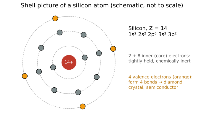
Quantum mechanics allows electrons only certain energies. They fill shells (n = 1, 2, 3 …) subdivided into orbitals labelled s, p, d, f, holding 2, 6, 10, 14 electrons respectively. Filling from lowest energy up gives the electron configuration:
The ten inner electrons ([Ne] core) are tightly bound and chemically inert; the four valence electrons (3s² 3p²) do all the chemistry and all the electronics.
The periodic table as a map
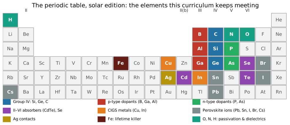
Elements are arranged by Z in rows (periods, the outermost shell) and columns (groups, same number of valence electrons and so similar chemistry). For PV, the "semiconductor neighbourhood" around silicon matters most:
| Group | Valence e⁻ | PV role |
|---|---|---|
| III (B, Al, Ga, In) | 3 | p-type dopants in Si; Ga/In in CIGS; Al in rear contacts and Al₂O₃ passivation |
| IV (C, Si, Ge, Sn) | 4 | Si absorber; Ge substrate for space III–V cells; Sn in some perovskites |
| V (N, P, As) | 5 | P n-type dopant (POCl₃ diffusion, TOPCon poly-Si); N in SiNₓ; As in GaAs |
| VI (O, S, Se, Te) | 6 | O in SiO₂/Al₂O₃ and as an impurity in Cz-Si; Se in CIGS; Te in CdTe |
| II (Zn, Cd) | 2 | Cd in CdTe; Zn in ZnO/buffer layers |
| Halogens (Cl, Br, I) | 7 | chlorosilane chemistry; perovskite X-site |
Why dopants work: a phosphorus atom sitting in a silicon site uses four electrons to bond and has a fifth left over, loosely held — it is easily freed to conduct (n-type). Boron has only three, leaving a missing bond — a hole (p-type). (SOL 201 makes this quantitative.)
Periodic trends
- Atomic radius grows down a group (more shells) and shrinks across a period (more nuclear charge pulling the same shell).
- Ionisation energy (energy to remove an electron; Si: 8.15 eV) grows across a period and falls down a group.
- Electronegativity — how strongly an atom pulls shared electrons — grows toward the upper right (F is highest). It decides bond type (Unit 2).
These trends explain, for example, why the band gap shrinks from C (5.5 eV) to Si (1.12 eV) to Ge (0.66 eV) down group IV: bigger atoms, longer and weaker bonds (Unit 2).
Abundance
Silicon is the second most abundant element in Earth's crust (about 28 % by mass, after oxygen at about 46 %), almost entirely as silica and silicates — sand, quartz, granite. Abundance is not the bottleneck; purity and energy are (Unit 8; SOL 301). Contrast tellurium and indium, which are rare by-products of copper and zinc mining — a materials-supply issue for CdTe and CIGS (SOL 305/404).
Moles and counting atoms
One mole is \(6.022 \times 10^{23}\) particles (Avogadro's number); its mass in grams equals the atomic mass (28.0855 g for Si).
Worked example 1 — atoms in a wafer
A 182 mm × 182 mm wafer, 130 µm thick (ignoring the clipped corners): volume \(= 18.2 \times 18.2 \times 0.013 = 4.31\) cm³. Mass \(= 4.31 \times 2.329 = 10.0\) g. Moles \(= 10.0/28.09 = 0.357\). Atoms \(= 0.357 \times 6.022\times10^{23} = 2.15 \times 10^{23}\).
Worked example 2 — grams per watt
That wafer becomes a cell of about 8.3 W (SOL 101 Unit 1): \(10.0/8.3 \approx 1.2\) g of wafer silicon per watt. Including the silicon lost as sawing kerf and in ingot tops/tails, industry-wide polysilicon use was about 2.0 g/Wp in 2024 (Fraunhofer ISE Photovoltaics Report, 2026) — down from about 16 g/Wp in 2004.
Worked example 3 — what does 'ppm' mean in silicon?
Silicon has \(5.0 \times 10^{22}\) atoms/cm³. One part per million atomic (ppma) \(= 5 \times 10^{16}\) cm⁻³; one part per billion (ppba) \(= 5\times10^{13}\) cm⁻³. A typical n-type wafer doping of \(5\times10^{15}\) cm⁻³ is just 0.1 ppma — semiconductors are controlled at astonishingly low concentrations.
Common misconceptions
Misconceptions
- "Electrons orbit like planets." The shell picture is a bookkeeping cartoon; electrons occupy orbitals (probability clouds) with definite energies.
- "Purer silicon is needed because silicon is rare." Silicon is abundant; purity is needed because tiny impurity levels (ppb) ruin electronic properties.
- "Dopants are impurities that make silicon worse." Dopants are deliberate impurities that make silicon useful; unwanted metals are the harmful ones.
What this means for manufacturing and the job
- Dopant sources (POCl₃ for P, BBr₃/BCl₃ for B; Ga in the melt for p-type ingots) come straight from groups III and V (SOL 301/302).
- Purity grades (9N for solar polysilicon = 99.9999999 %) and contamination specs (ppb/ppt metals) are periodic-table numbers (SOL 301/402).
- Material supply questions (Ag, In, Te, Bi) appear in roadmaps and job interviews alike (SOL 404).
Review questions
1. Write the electron configuration of phosphorus (Z = 15). How many valence electrons?
[Ne] 3s² 3p³ — five valence electrons.
2. Why does boron make silicon p-type?
It has three valence electrons, one short of the four bonds in the lattice; the missing electron (a hole) can move and carry positive charge.
3. How many atoms are in 1 g of silicon?
(1/28.0855) × 6.022 × 10²³ = 2.14 × 10²² atoms.
4. Convert 1 ppba of iron in silicon into atoms per cm³.
5.0 × 10²² × 10⁻⁹ = 5 × 10¹³ cm⁻³.
5. Why does band gap decrease from C to Si to Ge?
Going down group IV, atoms get larger, bonds longer and weaker, so the energy separating bonding (valence) and antibonding (conduction) states shrinks.
Sources
- Any general chemistry text (e.g., Zumdahl, Chemistry); IUPAC atomic weights; NIST isotopic compositions.
- CRC Handbook (ionisation energy, crustal abundance).
- Fraunhofer ISE, Photovoltaics Report (14 July 2026): silicon use per Wp.