Unit 3 — Crystal Structures and Miller Indices
Big idea. In a crystal, atoms repeat in a perfect 3-D pattern. Silicon's pattern — diamond cubic — follows from its four tetrahedral bonds. GaAs and CdTe use the same geometry with two atom types (zinc blende); CIGS doubles it (chalcopyrite); halide perovskites use a different, cage-like ABX₃ structure. Miller indices name crystal planes — essential because wafers are cut on (100) and alkaline etching reveals {111} pyramids.
Learning objectives
- Define lattice, basis, unit cell and lattice constant.
- Describe the diamond-cubic structure and compute silicon's atom density and density from its lattice constant.
- Describe zinc blende, chalcopyrite and perovskite structures and name PV materials in each.
- Use Miller indices for planes and directions; compute angles and spacings between planes.
- Explain why (100) wafers texture into {111}-faced pyramids and cleave along {111}/{110}.
Why this matters
Crystal orientation decides how wafers are grown (⟨100⟩ Czochralski seeds), how they break, how they etch (pyramid texture), and how films grow on them (epitaxy). X-ray diffraction, a standard metrology tool, reads crystal structure directly.
Lattice, basis, unit cell
A crystal = a lattice (a regular array of points) + a basis (the group of atoms placed at each point). The smallest repeating box that shows the full symmetry is the unit cell; its edge length is the lattice constant \(a\). Many structures relevant here are built on the face-centred cubic (FCC) lattice: points at the cube corners and face centres.
Diamond cubic: silicon
Silicon's structure is an FCC lattice with a two-atom basis at (0,0,0) and (¼,¼,¼)a. Equivalently, two interpenetrating FCC lattices offset by a quarter of the body diagonal. Each atom has four nearest neighbours at the corners of a tetrahedron — exactly the sp³ bonding of Unit 2.
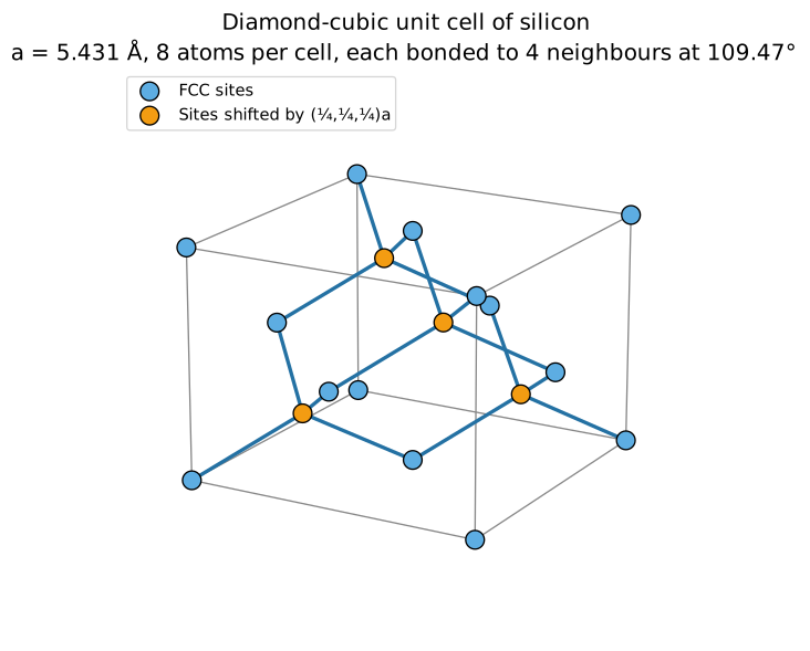
Counting atoms in the cubic cell: 8 corners × ⅛ + 6 faces × ½ + 4 inside = 8 atoms.
Worked example 1 — silicon's atom density and density from geometry
\(a = 5.431\) Å \(= 5.431\times10^{-8}\) cm, so \(a^3 = 1.602\times10^{-22}\) cm³. Atom density \(= 8/a^3 = 4.99 \times 10^{22}\) cm⁻³ (the "5 × 10²²" used everywhere). Mass density \(= \dfrac{8 \times 28.0855\ \text{g/mol}}{6.022\times10^{23} \times 1.602\times10^{-22}\ \text{cm}^3} = 2.329\) g/cm³ ✔ (matches the measured value). Nearest-neighbour distance \(= \sqrt{3}a/4 = 2.35\) Å.
The diamond structure is surprisingly empty — only about 34 % of space is filled by touching spheres (vs 74 % for FCC metals) — because directional bonds, not packing, dictate geometry.
Zinc blende: GaAs, CdTe
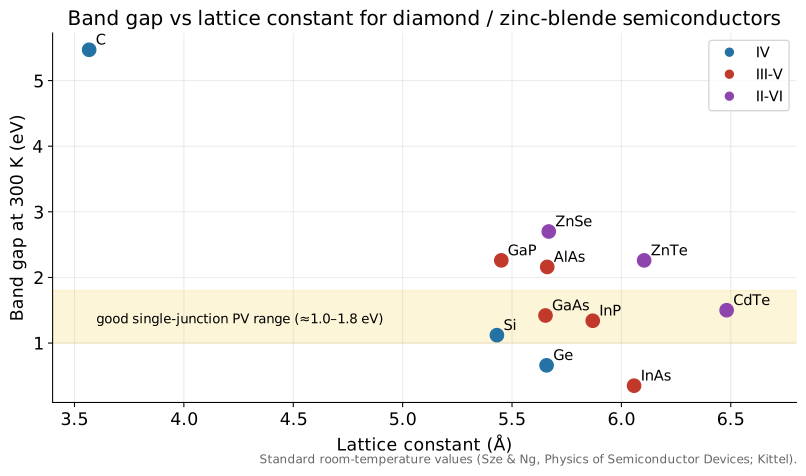
Put one element on the FCC sites and another on the (¼,¼,¼) sites: zinc blende (sphalerite). Every Ga is bonded to four As and vice versa. GaAs (a = 5.653 Å), CdTe (6.481 Å), InP, ZnSe use it. Average valence is still four electrons per atom (III+V or II+VI), keeping the tetrahedral bonding.
Chalcopyrite: CuInSe₂ / CIGS
Replace the group-II site of zinc blende alternately by Cu (group I) and In or Ga (group III) in an ordered way: the cell doubles along one axis (tetragonal). This chalcopyrite structure is CuInSe₂ / Cu(In,Ga)Se₂ (CIGS). Varying Ga/(In+Ga) tunes the band gap from about 1.0 eV (CuInSe₂) to about 1.7 eV (CuGaSe₂) — standard literature range (SOL 305).
Perovskite ABX₃
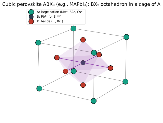
Perovskites (named after the mineral CaTiO₃) have formula ABX₃: a small B cation (Pb²⁺ or Sn²⁺ in solar perovskites) sits inside an octahedron of X anions (I⁻, Br⁻, Cl⁻); the octahedra share corners, and a large A cation (methylammonium MA⁺, formamidinium FA⁺, Cs⁺) fills the cages between them. Whether a combination forms a perovskite is predicted by the Goldschmidt tolerance factor
with stable 3-D perovskites roughly for \(0.8 \lesssim t \lesssim 1.0\). MAPbI₃ has a band gap of about 1.55–1.6 eV; mixing Br raises it toward the ~1.65–1.75 eV wanted for silicon tandem top cells.
Band gap vs lattice constant
Miller indices
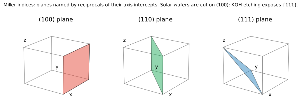
To name a plane: (1) find where it cuts the x, y, z axes in units of \(a\); (2) take reciprocals; (3) clear fractions to the smallest integers → \((hkl)\). A plane parallel to an axis has intercept ∞ → index 0. Negative indices carry a bar.
- (100): cuts x at 1, parallel to y and z — a cube face.
- (110): cuts x and y at 1 — a diagonal plane.
- (111): cuts x, y, z at 1 — the plane across three cube corners.
Notation: \((hkl)\) one plane; \(\{hkl\}\) the family of equivalent planes; \([hkl]\) a direction; \(\langle hkl\rangle\) the family of equivalent directions. In cubic crystals, \([hkl]\) is perpendicular to \((hkl)\).
Two formulas you will use:
In words: plane spacing shrinks for higher indices; the angle between planes is the angle between their normal vectors.
Worked example 2 — the pyramid angle
Angle between (100) and (111): \(\cos\theta = 1/(\sqrt{1}\sqrt{3}) = 0.577\) → 54.74°. Alkaline (KOH/NaOH) etching attacks {100} much faster than {111}, so a (100) wafer etches into square-based pyramids whose four faces are {111} planes inclined at 54.74° (Unit 8). Why {111} is slow: each surface atom there has three bonds into the crystal and only one exposed, versus two and two on {100} (Seidel et al. 1990 explanation).
Worked example 3 — X-ray diffraction peak of silicon
Bragg's law \(n\lambda = 2d\sin\theta\). For Si (111): \(d = 5.431/\sqrt{3} = 3.136\) Å. With Cu Kα X-rays (\(\lambda = 1.5406\) Å): \(\sin\theta = 1.5406/(2\times3.136) = 0.2457\) → \(\theta = 14.22°\) → the diffractometer shows a peak at \(2\theta = 28.44°\), the textbook silicon reference peak.
Cleavage
Silicon cleaves most easily along {111} planes, and also along {110}. A (100) wafer scribed and snapped breaks along ⟨110⟩ directions — the straight, perpendicular cleavage lines you will see in Lab 102-B. Wafer flats/notches mark crystal orientation for this reason.
Common misconceptions
Misconceptions
- "A unit cell is a molecule." It is a repeating geometric box; atoms on corners and faces are shared with neighbouring cells.
- "Pyramids are etched by a mask." Random-pyramid texture forms without masks because of etch-rate anisotropy.
- "(100) and [100] are the same thing." One is a plane, the other a direction (they are perpendicular in cubic crystals).
- "Perovskite means one material." It is a structure type; solar perovskites are a family of compositions.
What this means for manufacturing and the job
- Cz ingots are pulled from ⟨100⟩ seeds so wafers are (100) for texturing (SOL 301).
- Wafer breakage and laser/cleave cutting (half-cells) follow crystal planes (SOL 304/402).
- XRD characterises films (perovskite phase purity, CIGS, TCO crystallinity) (SOL 401).
- Epitaxy (lattice matching) governs III–V and tandem growth (SOL 305).
Review questions
1. Miller indices of a plane with intercepts x = 1, y = 2, z = ∞?
Reciprocals 1, ½, 0 → ×2 → (210).
2. Spacing of Si (220) planes?
5.431/√8 = 1.920 Å.
3. Angle between (100) and (110)?
cos θ = 1/√2 → 45°.
4. How many atoms are in the diamond-cubic unit cell, and why?
8: 8 corners × ⅛ = 1, 6 faces × ½ = 3, plus 4 interior atoms.
5. Compute the tolerance factor for CsPbI₃ using r(Cs⁺) = 1.88 Å, r(Pb²⁺) = 1.19 Å, r(I⁻) = 2.20 Å (Shannon radii, approximate).
t = (1.88 + 2.20)/(1.414 × (1.19 + 2.20)) = 4.08/4.79 ≈ 0.85 — at the edge of stability; indeed cubic CsPbI₃ tends to convert to a non-perovskite phase at room temperature.
Sources
- Kittel, Introduction to Solid State Physics, ch. 1; Callister ch. 3.
- Lattice constants and band gaps: Sze & Ng; Ioffe Institute semiconductor database.
- Seidel et al., J. Electrochem. Soc. 137, 3612 (1990) — anisotropic etching of Si in KOH.
- Cu Kα wavelength: standard value 1.5406 Å.
- Shannon, Acta Cryst. A32, 751 (1976) — ionic radii (values approximate here).